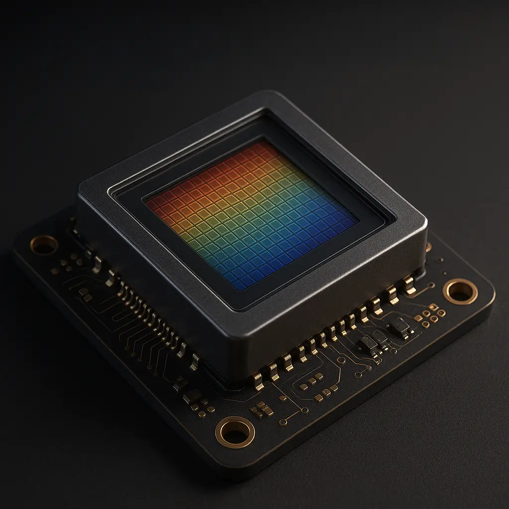
An innovation in precision imaging where every photon counts
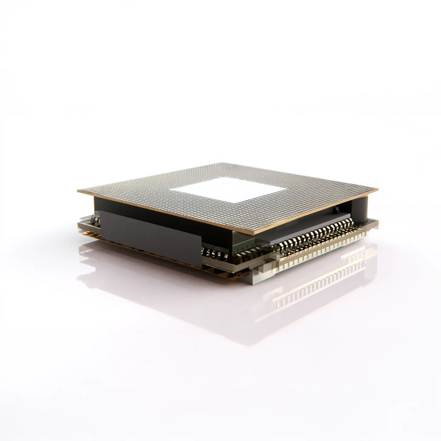
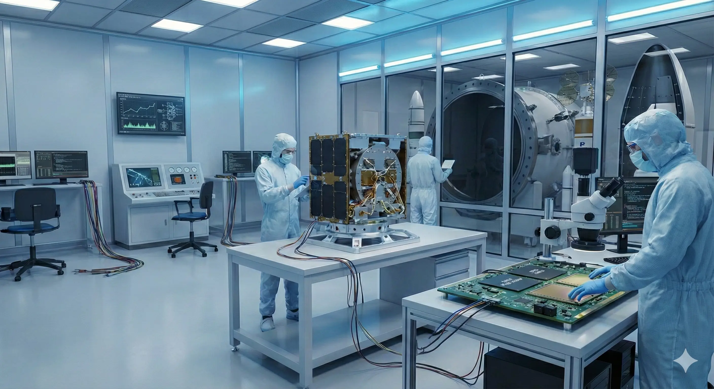
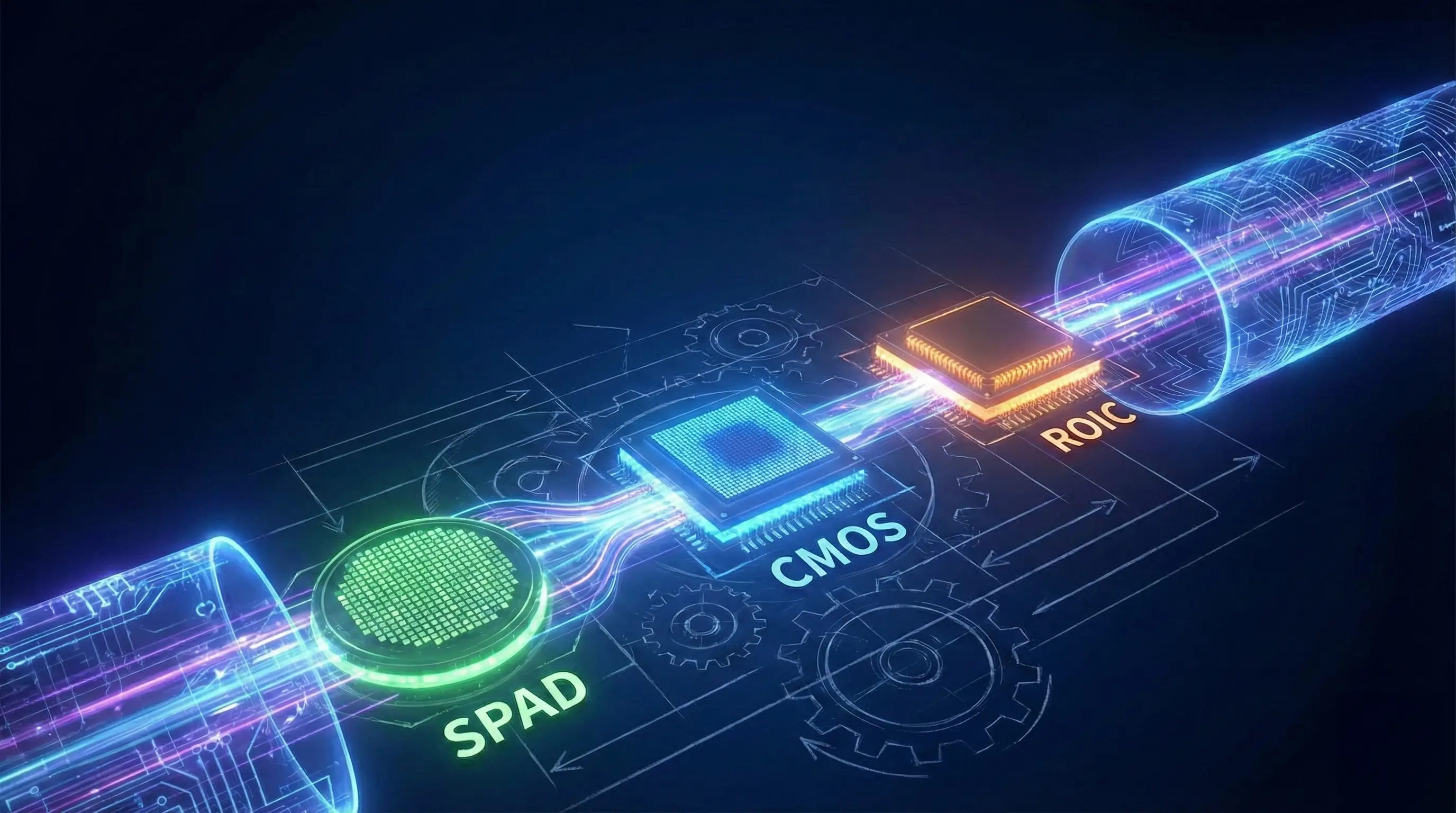
Engineering custom imaging architectures for science, industry, and defense. From advanced CMOS pixel design to photon-counting SPAD arrays.


Have Questions?
Have Any Questions?
We’re happy to walk through details, timelines, or next steps whenever you’re ready.
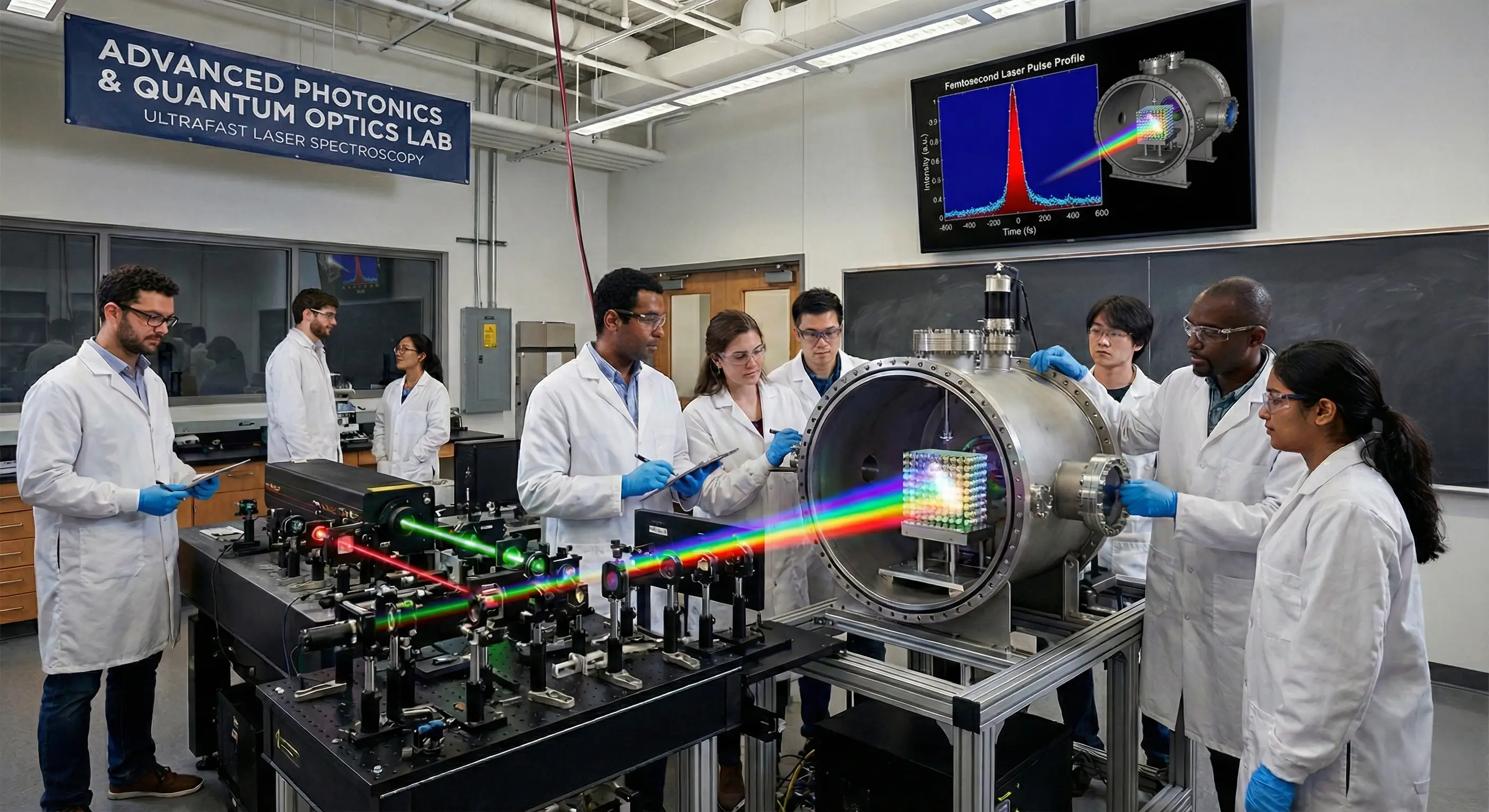
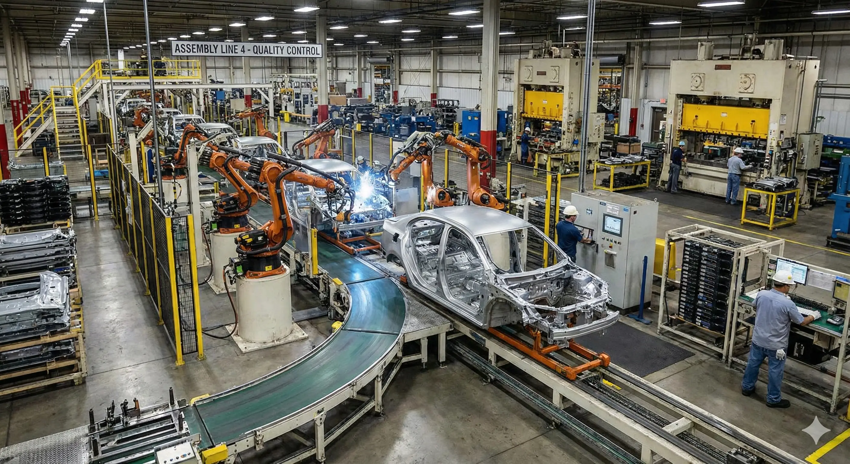
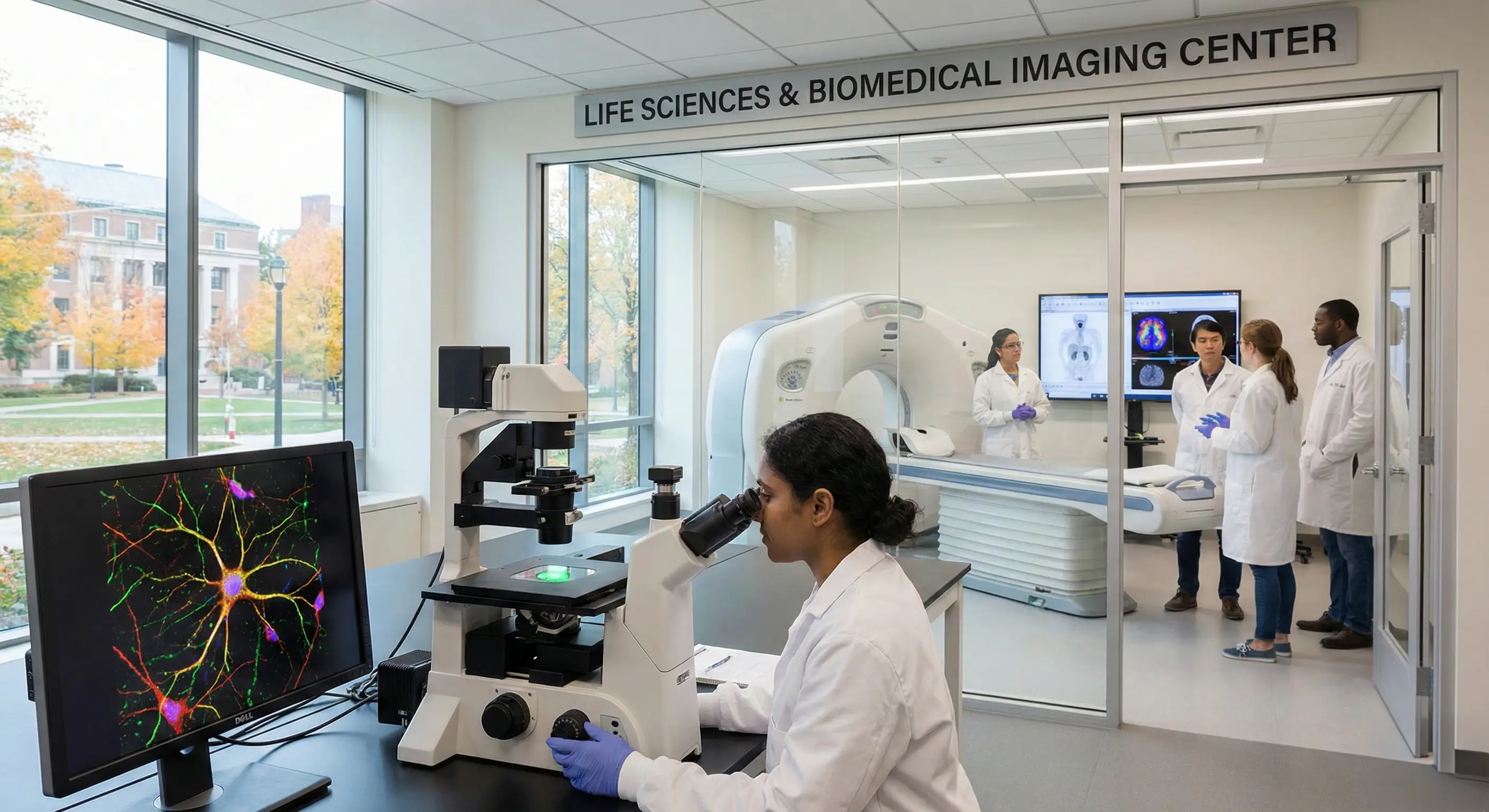
We focus on complex imaging and sensor challenges that operate at or near physical limits. This includes photon-limited environments, high dynamic range sensing, low-noise architectures, and systems where accuracy and signal integrity directly impact outcomes.
Our process is milestone-driven and collaborative. We begin with your high-level requirements, then carefully translate them into detailed IC design specifications and product performance targets.
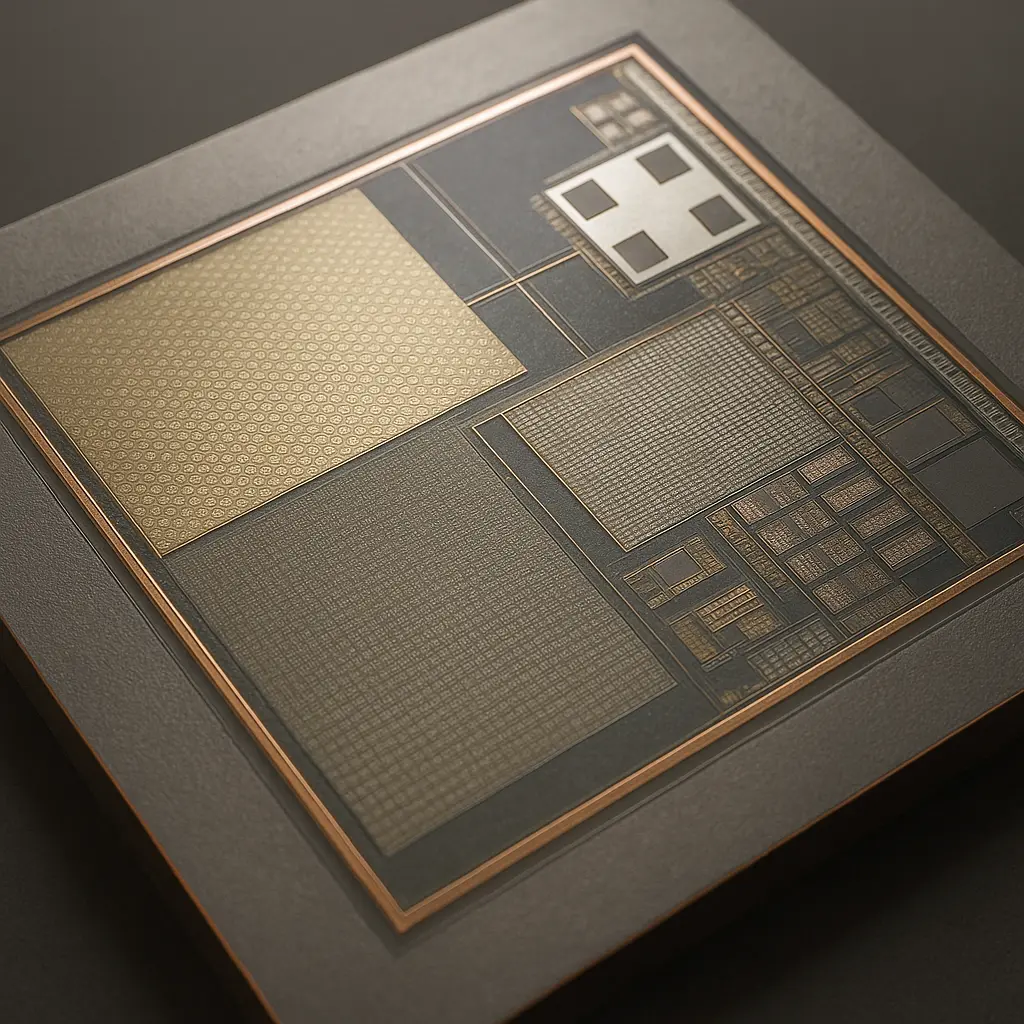
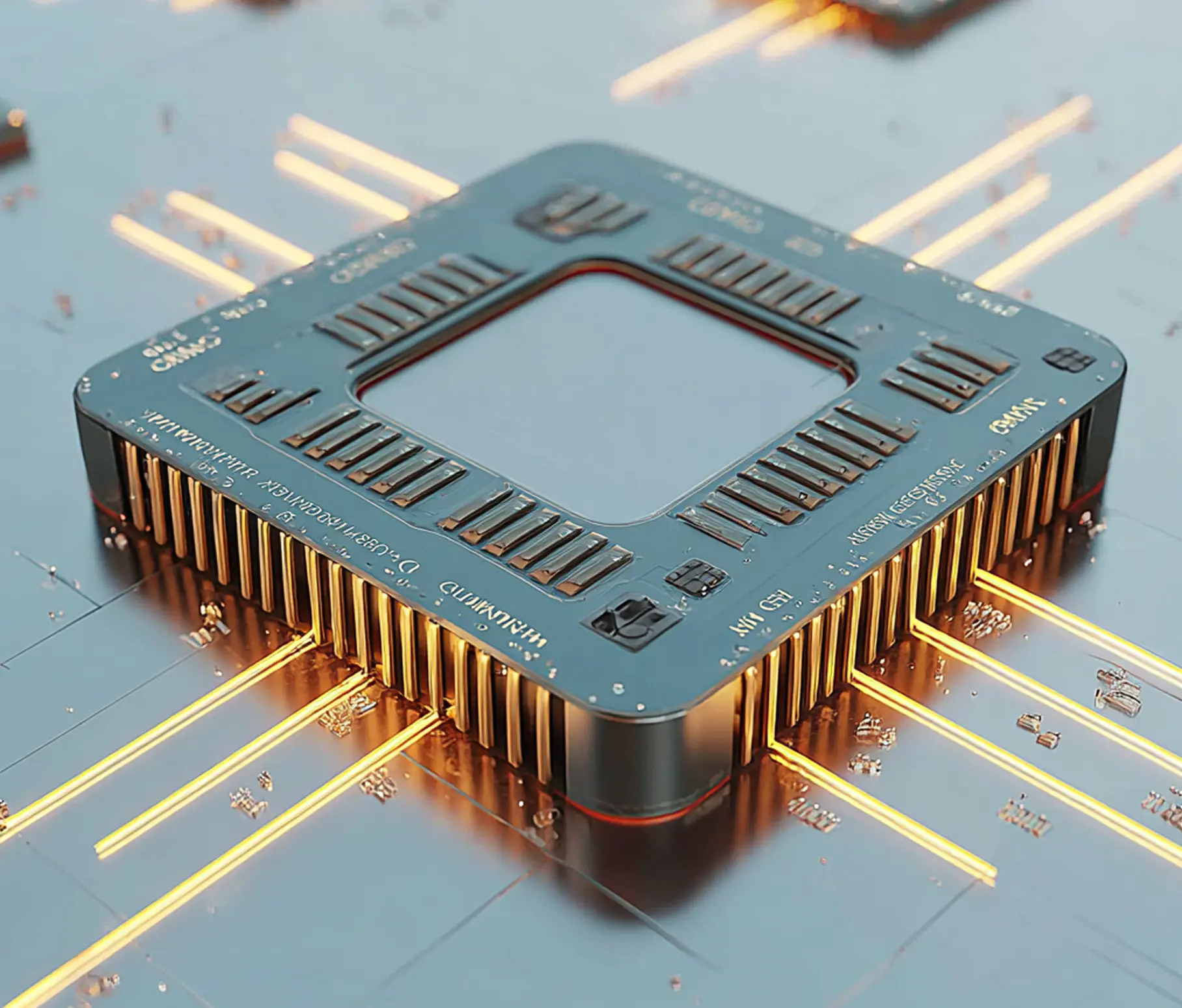
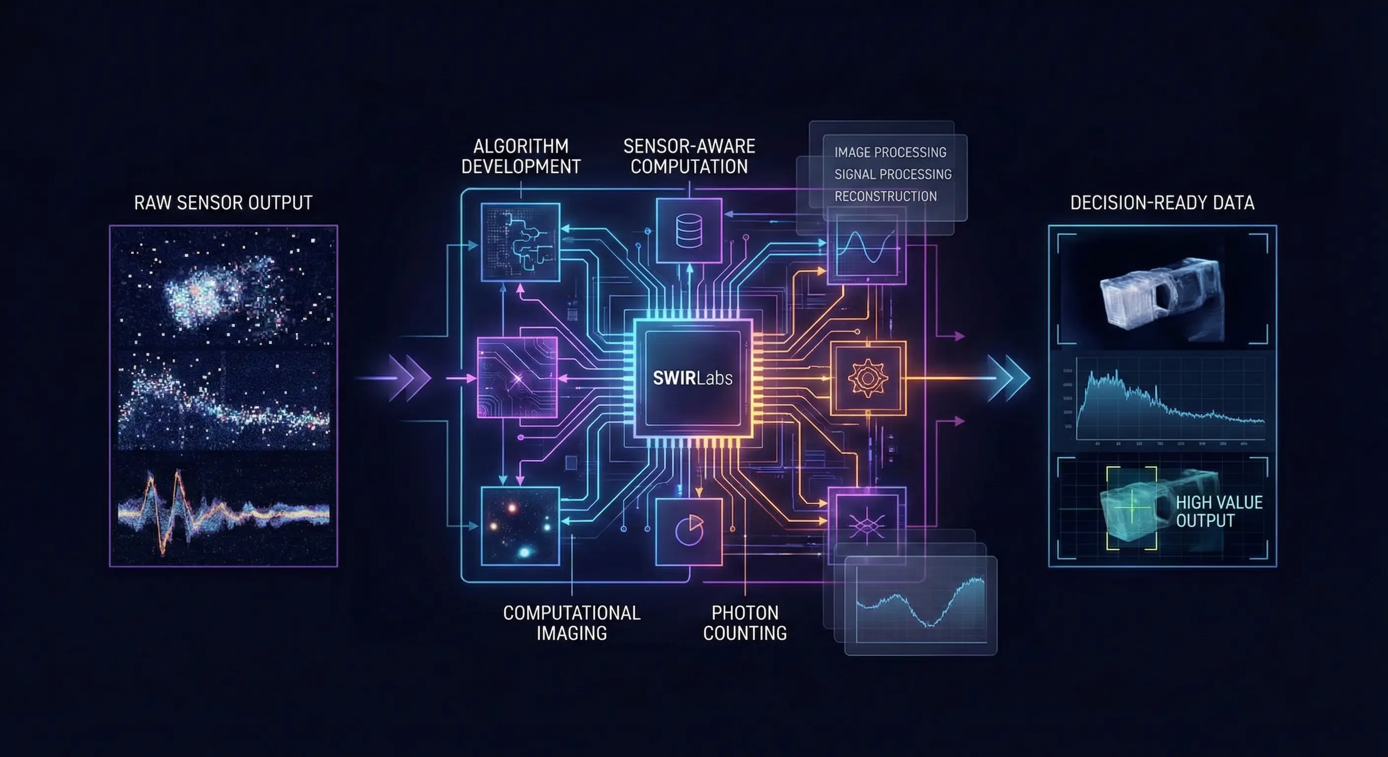
Our work is driven by a system-level understanding of imaging physics, sensor design, and computational processing. Rather than optimizing isolated components, we engineer solutions that balance performance, scalability, and manufacturability across the full imaging pipeline.
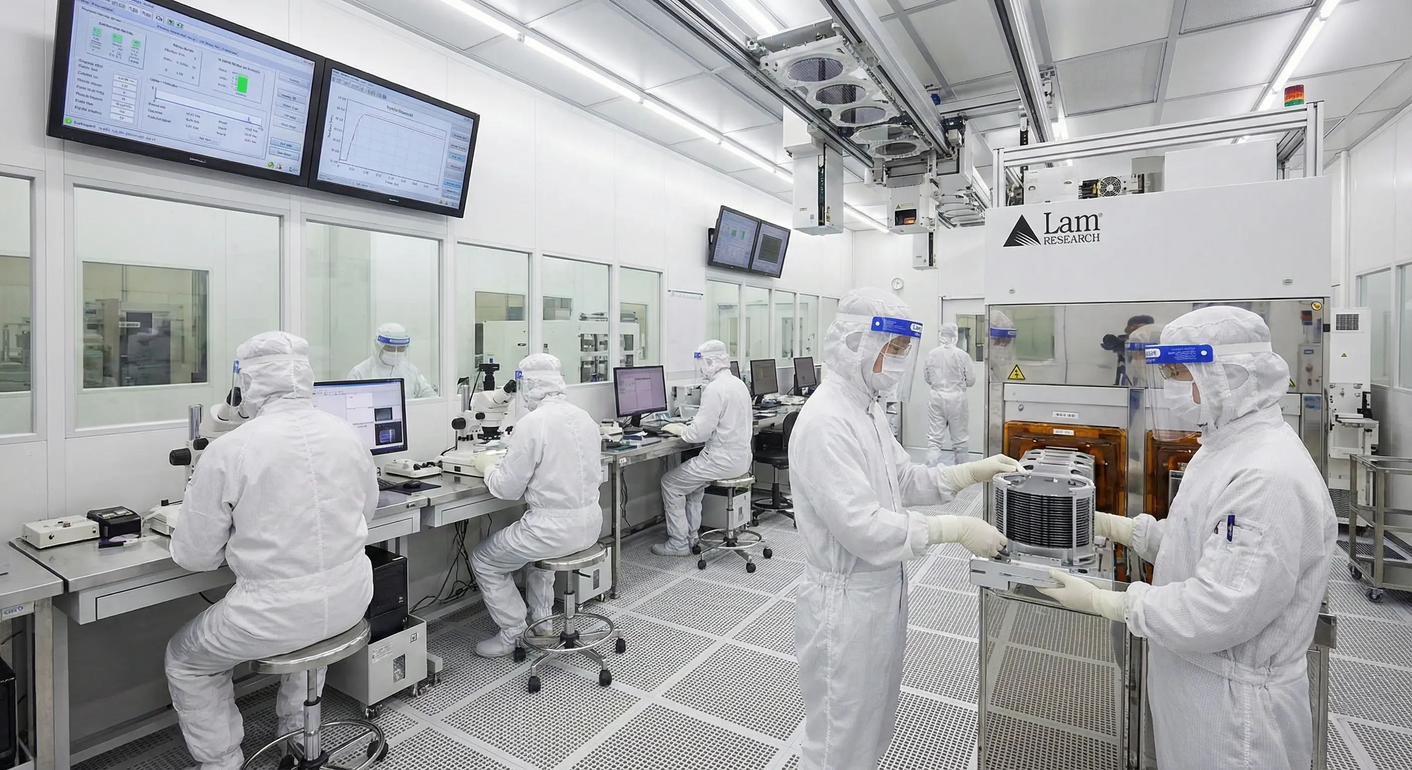
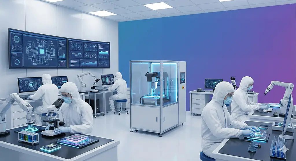
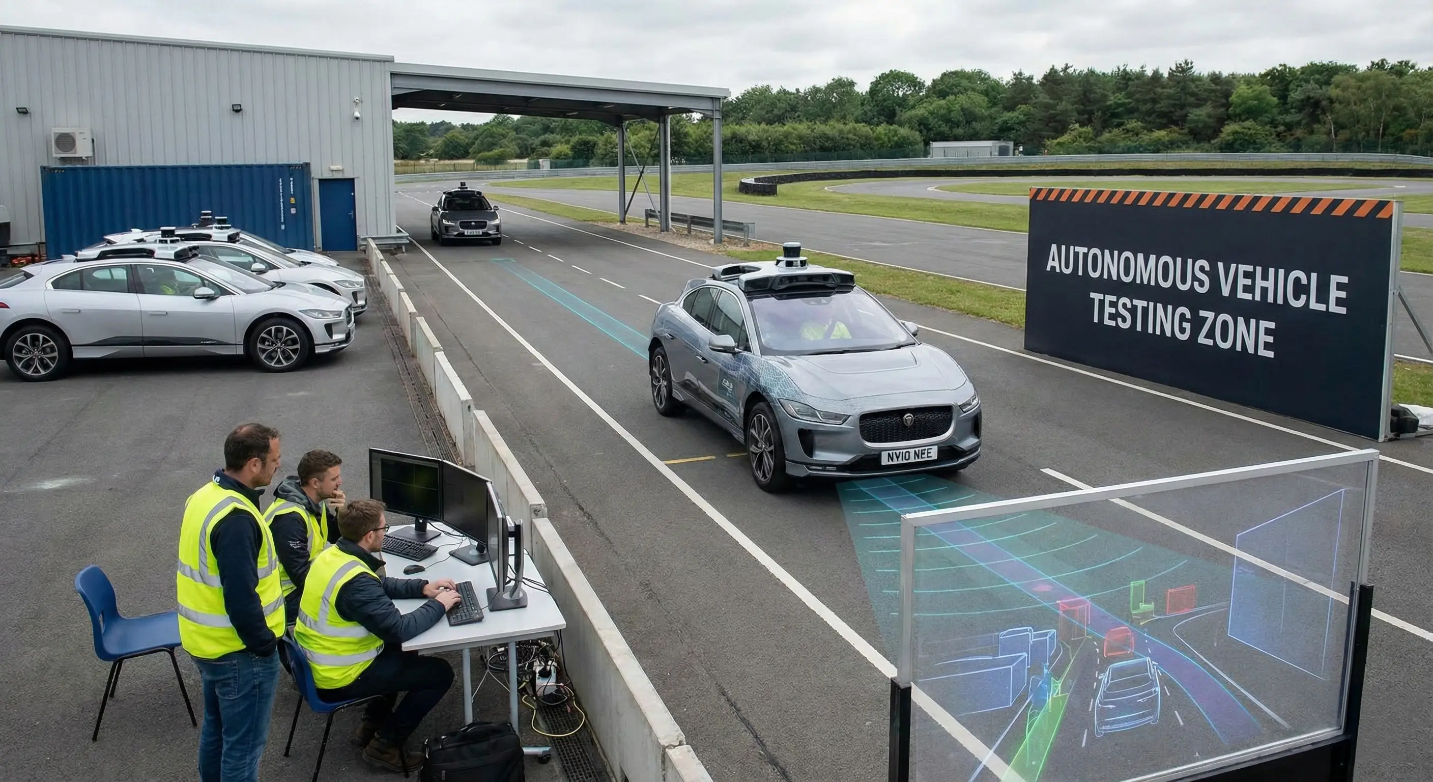
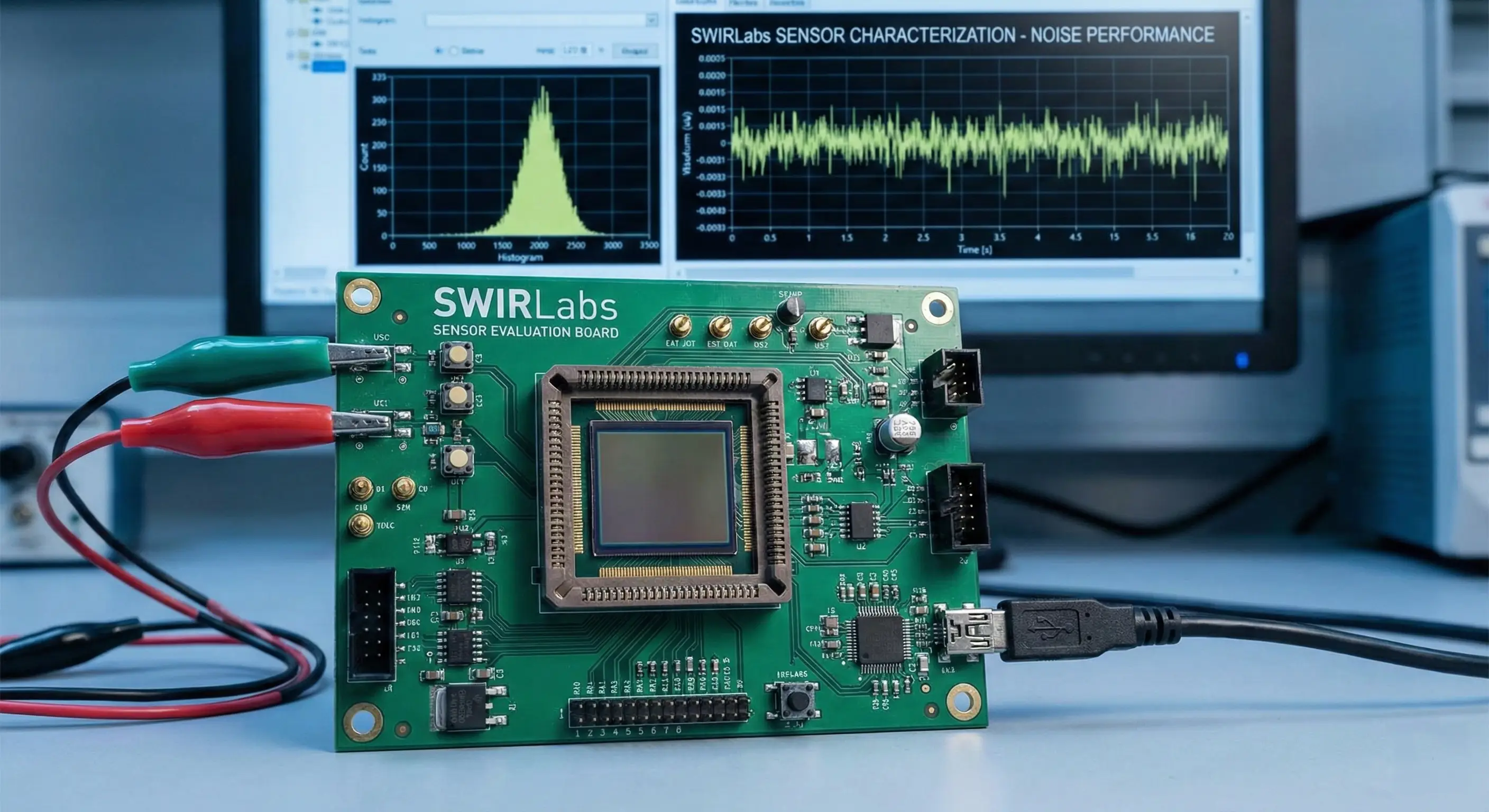
We emphasize validation and characterization early to ensure prototypes translate into deployable systems. This includes performance testing, design trade-offs, and alignment with operational, environmental, and manufacturing constraints.
Yes. Many of the systems we work on do not have off-the-shelf solutions. We specialize in custom architectures, novel imaging approaches, and tailored designs driven by specific mission or research requirements.
We use industry-leading CAD tools from Siemens, Cadence, and Synopsys, and collaborate with world-class semiconductor fabrication partners to bring advanced designs to life.
Absolutely. We’d love to learn more about your image sensor project, understand your industry needs, and explore how we can help you achieve your goals.